I2C-Master core introduction
I2C is a two-wire, bi-directional serial bus that provides a simple and efficient method of
data exchange between devices. It is most suitable for applications requiring occasional
communication over a short distance between many devices. The I2C standard is a true
multi-master bus including collision detection and arbitration that prevents data
corruption if two or more masters attempt to control the bus simultaneously.
The interface defines 3 transmission speeds:
Normal: 100Kbps
Fast: 400Kbps
High speed: 3.5Mbps
Only 100Kbps and 400Kbps modes are supported directly. For High speed special IOs
are needed. If these IOs are available and used, then High speed is also supported.
FEATURES
? Compatible with Philips I2C standard
? Multi Master Operation
? Software programmable clock frequency
? Clock Stretching and Wait state generation
? Software programmable acknowledge bit
? Interrupt or bit-polling driven byte-by-byte data-transfers
? Arbitration lost interrupt, with automatic transfer cancelation
? Start/Stop/Repeated Start/Acknowledge generation
? Start/Stop/Repeated Start detection
? Bus busy detection
? Supports 7 and 10bit addressing mode
? Operates from a wide range of input clock frequencies
? Static synchronous design
? Fully synthesizable
2.1 Core Parameters

2.1.1 ARST_LVL
The asynchronous reset level can be set to either active high (1’b1) or active low (1’b0).
2.2 WISHBONE interface signals
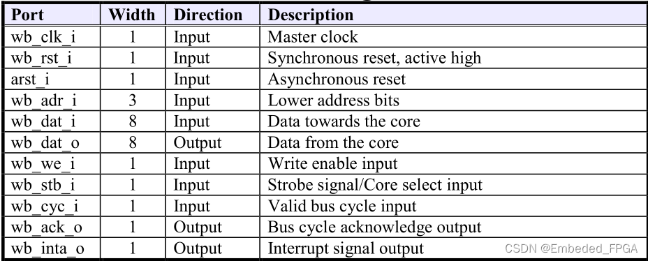
The core features a WISHBONE RevB.3 compliant WISHBONE Classic interface. All output signals are registered. Each access takes 2 clock cycles.
arst_i is not a WISHBONE compatible signal. It is provided for FPGA implementations.
Using [arst_i] instead of [wb_rst_i] can result in lower cell-usage and higherperformance, because most FPGAs provide a dedicated asynchronous reset path. Use either [arst_i] or [wb_rst_i], tie the other to a negated state.
2.3 External connections
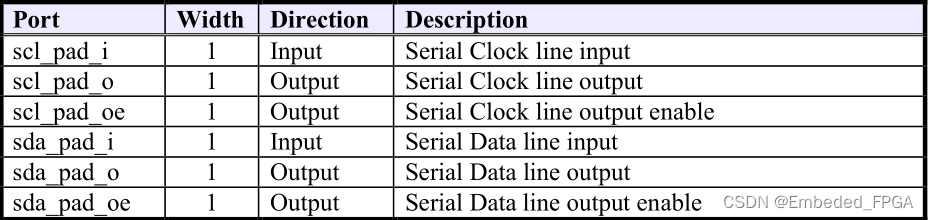
The I2C interface uses a serial data line (SDA) and a serial clock line (SCL) for datatransfers. All devices connected to these two signals must have open drain or open collector outputs. Both lines must be pulled-up to VCC by external resistors.
The tri-state buffers for the SCL and SDA lines must be added at a higher hierarchical level. Connections should be made according to the following figure:
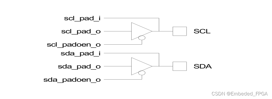
For FPGA designs the compiler can automatically insert these buffers using the following
VHDL code:
scl <= scl_pad_o when (scl_padoen_oe = ‘0’) else ‘Z’;
sda <= sda_pad_o when (sda_padoen_oe = ‘0’) else ‘Z’;
scl_pad_i <= scl;
scl_pad_i <= sda;
Verilog code:
assign scl = scl_padoen_oe ? 1’bz : scl_pad_o;
assign sda = sda_padoen_oe ? 1’bz: sda_pad_o;
assign scl_pad_i = scl;
assign sda_pad_i = sda;
本文来自互联网用户投稿,该文观点仅代表作者本人,不代表本站立场。本站仅提供信息存储空间服务,不拥有所有权,不承担相关法律责任。 如若内容造成侵权/违法违规/事实不符,请联系我的编程经验分享网邮箱:veading@qq.com进行投诉反馈,一经查实,立即删除!